Printed circuit boards make the foundation of every electronic and digital device and are the backbone of electronics like smartphones, laptops, digital watches, microwaves, car parts, and many more. PCBs hold great importance in today’s digital world, and due to their large variety of uses, their demand has increased. All of the multinational industries and organizations want high-quality PCB boards for their electronic devices.
Two Main PCB Assembly Methods
You might be familiar with the term printed circuit boards, but have you ever thought about how PCBs have become a part of our everyday life? There are three crucial stages involved in the manufacturing and assembling of PCB boards. You have to start with the design of the boards; it requires a schematic diagram, PCB Gerber files and bill of materials. Then, there is the fabrication of the printed circuit boards, and lastly, we mount the components on the boards; this process is called the assembly of the board.
A printed circuit board without the assembly of the components on its surface to become a functional PCB. The assembly of the board can be done with two methods, i.e., through-hole technology and surface mount technology. Through-hole assembly is the assembly method used first and it is still widely used. The Surface mount technology is a relatively modern method. The proper functionality of the electronic and digital devices is highly reliable on the high quality PCBs.
Seven PCB Assembly Process Steps
If you are a beginner and want to hold a grip on the assembly process in PCB board manufacturing, then this article is going to provide you with a step-by-step guide to PCB assembly. Let’s examine the important steps in PCB assembly manufacturing.
PCB Production or Sourcing
But before you start PCB assembly, you must have PCB bare boards first, which is used to assemble the components onto them. This is the first task you need to do in PCB assembly steps. You need to produce board boards if you can, or outsource PCBs to PCB manufacturers. PCB board including the following basic components and materials:
- Base material: to hold the components and traces on the boards, the manufacturers use supporting material, substrate, such as FR4, metal core, PTFE, ceramic., etc.
- Copper: you must be aware of the highly conductive quality of copper; that’s why it is used in PCBs for the smooth flow of electric current.
- Solder mask: to coat all of the components with epoxy, a technique called solder mask is used, except for the card-edge connectors.
- Silkscreen: a silkscreen is typically a digitally printed circuit board and helps you to recognize the mistakes in the assembly and position of the components, where they should be placed on the board.
- Annular ring: you may notice a copper ring around the holes on the boards; it is the annular ring.
- Trace: a pathway through which the electrical signals travel is trace. It is usually a copper structure for the smooth flowing of electrical signals.
- Holes: there are different kinds of holes, such as PTH (plated through holes) and NPTH (non-plated through holes) . PTH are used to connect all copper layers, and also used to insert components pins. NPTH are used to be mounting holes.
Preparing Electronic Components as BOM
To start, firstly, you have to go through the list of bill of materials (BOM). Your bill of materials must include the knowledge of reference designators, component value, and quantity of the boards, manufacturer part number or the package.
Most of the manufacturers use the CAD machine to generate the BOM of the boards. You can put a design in the machine, and it will generate the spreadsheet or CSV file.
You must make a well-defined bill of materials to give clear instructions throughout the whole process of PCB assembly. However, the bill of materials can vary according to the type of assembly. An attractive bill of materials can be helpful in the right placement of the components on the boards, sourced components tracking, and finding out the components that have been wrongly placed. So BOM checking is also very import in PCB assembly steps.
Before PCB assembly, we need to prepare all the electronics components according to the BOM list. In the BOM, the components like resistors, capacitors, and fuses that would be mounted on the boards in the PCB assembly process using the through-hole or surface mount technology.
Applying Solder Paste
When we get PCBs and all components ready. Next comes the application of solder paste on the boards. In the solder paste applying process, stencils are always needed. A solder paste stencil is typically a metal sheet usually made up of steel or nickel. These solder paste stencils have holes in them, cut very accurately as per the design layout of the printed circuit boards. For the correct alignment of the PCB boards and stencil sheets, they fit together firmly, and after that, a solder paste is applied to them.
A solder paste often comes in green bottles in which the solder paste is held in the form of solder flux. A mixture of solder paste would contain different metals like tin and lead, but now there is a demand for lead-free PCB circuit boards in the market, so lead-free solder paste is recommended for PCB assembly.
The solder paste may contain different amounts of various metals like tin, copper, or silver. However, some of the solder pastes include other metals as well. The amount of these components in the mixture may vary according to the combination.
It is also possible that you can apply a solder mask on the boards without the help of a stencil sheet. For this purpose, you have to use a smaller spatula and a dispenser syringe can be used.
Placement of the Components
The next and most critical step in the PCB assembly is the placement of the components on the boards after you have applied the solder paste. Two types of methods are used for the placement of the components on board; if you have opted for the through-hole technology, then the placement would be done by hand or automatic PTH components placement machine.
The tweezers are typically used for manual placement of the components. PTH components placement is suitable for mass production.
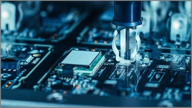
On the other hand, in surface mount technology, cutting-edge machines are used for this purpose. A very renowned machine called pick-and-place has been used by various large factories and industries to directly mount the components on board. The use of technology reduces the chances of human errors.
Component placement is one of the most important PCB assembly process steps, since any small error will lead to failure on a whole batch of PCBs.
Components Soldering
When components are placed on the PCB boards, we need to solder the components permanently by tin. These are three methods: reflow soldering for SMT assembly, wave soldering for PTH assembly and iron soldering for manual soldering.
- Reflow soldering: if you have picked up the surface mount technology, then after passing through the pick-and-place machine, the boards with components are put in a conveyer belt which passes through the oven to melt the solder paste through its heat. However, there are also reflow guns and a small heat bed for this purpose.
- Wave soldering: if you have opted for the through-hole assembly (the best option for beginners), then you can mount the components on board manually in a process called wave soldering.
- Iron soldering: Most commonly, a soldering iron is used for this purpose. You may need an iron rod of 30 watts. Make sure to use enough solder and heat it beyond its melting point.
Inspection and Testing
At the end, make sure there are no errors in the placement of the components, and none of the components should be misplaced. To check the functionality and quality of the boards, large industries use various types of tests like functional tests, visual tests, electrical tests, automated optical inspections, in-circuit testing methods, burn-in testing, and some others.
Inspections and testings are also critical PCB assembly process steps, since no PCB assembly company can assure 100% qualified products without proper quality checking.
Cleaning and Packaging
After the process of soldering has been done, make sure to clean the excess of the solder paste or any spillover flux or dirt. For this purpose, you can use solder wicks or isopropanol.
Packaging is also one of the very important PCB assembly process steps since the small electronic components can be damaged very easily in transportation. Hard cartons, bubble plastics and ESD bags are usually needed to protect the PCB boards from damage.
Conclusion
Assembly of the PCB boards requires a lot of hard work and patience. To make better quality products, always follow the procedure carefully. If you are a beginner, then the steps of the PCB assembly provided in this guide would be a great help for you.
 Join Daily Trust WhatsApp Community For Quick Access To News and Happenings Around You.